
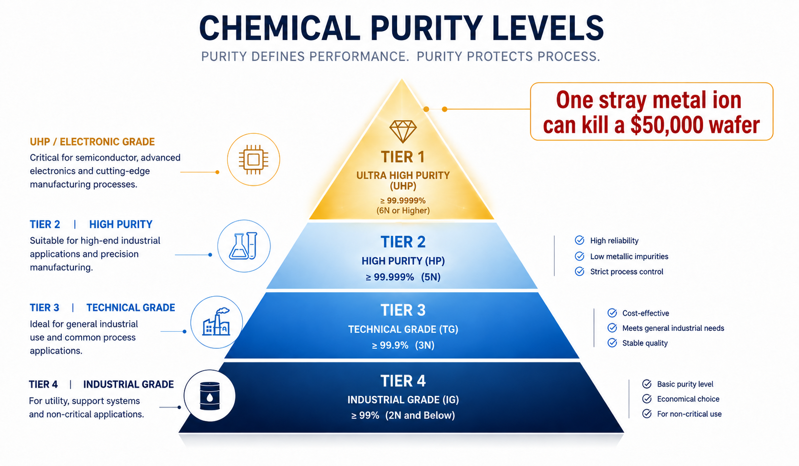
⚡ Executive Summary: Semiconductor manufacturing operates at parts per trillion (ppt) purity. One stray metal ion can kill a $50,000 wafer. Pump materials must resist aggressive chemicals (HF, H₂SO₄, H₂O₂) while contributing zero metal ion contamination.
When Parts Per Trillion Matter
Semiconductor fabs measure contamination in parts per trillion. Not parts per million. Not parts per billion. Parts per trillion.
A single iron or chromium atom leaching from a pump casing into the chemical stream can create a killer defect on a wafer worth $50,000+ with hundreds of chips. The pump must add nothing to the fluid. Period.
Critical Semiconductor Chemicals — Material Selection
Hydrofluoric Acid (HF) — 49%, High Purity
Used for SiO₂ etching and wafer cleaning. Extremely aggressive. Attacks most metals including stainless steels.
- Best: PTFE/PFA-lined pumps (ultra-high purity). Metal option: Hastelloy C-276 or Monel.
- 🚫 Avoid: Stainless steels, Titanium (attacked by HF), Alloy 20.
Sulfuric Acid (H₂SO₄) — 96%, High Purity
Used in piranha etch (with H₂O₂) and photoresist stripping.
- Best: Alloy 20 or Hastelloy C-276 (metal). PTFE/PFA-lined (ultra-high purity).
- Important: Electropolishing reduces ion leaching by 30-50%.
Hydrogen Peroxide (H₂O₂) — 30%, High Purity
RCA cleaning, piranha etch. Strong oxidizer.
- Best: 316SS, electropolished + passivated per ASTM A967.
Ammonium Hydroxide (NH₄OH) — 29%, High Purity
RCA SC-1 cleaning. Caustic — can cause SCC in some stainless steels.
- Best: 316SS or Nickel (CZ100).
CMP Slurries
Abrasive particles (silica, alumina, ceria) + chemically active solutions.
- Best: CD4MCuN (abrasion resistance + corrosion resistance). PTFE/PFA-lined (highest purity).
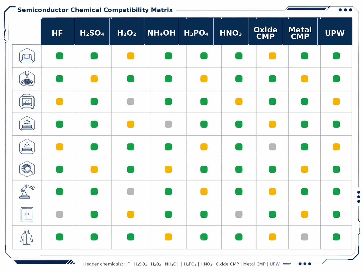
Semiconductor Chemical Compatibility Matrix
| Chemical | Conc. | Temp | Metal Pump Material | UHP Option |
|---|---|---|---|---|
| HF | 49% | Amb-120°F | Hastelloy C-276 / Monel | PTFE/PFA-lined |
| H₂SO₄ | 96% | Amb-250°F | Alloy 20 / Hastelloy C | PTFE/PFA-lined |
| H₂O₂ | 30% | Amb-160°F | 316SS (electropolished) | PTFE/PFA-lined |
| NH₄OH | 29% | Amb-140°F | 316SS / Nickel | PTFE/PFA-lined |
| H₃PO₄ | 85% | Amb-200°F | 316SS / Alloy 20 | PTFE/PFA-lined |
| HNO₃ | 70% | Amb-150°F | 316SS | PTFE/PFA-lined |
| CMP Slurry (oxide) | pH 10-11 | Amb-120°F | CD4MCuN | PTFE w/ hard-faced rings |
| CMP Slurry (metal) | pH 2-5 | Amb-120°F | CD4MCuN / Alloy 20 | PTFE w/ hard-faced rings |
| UPW | N/A | Amb-180°F | 316SS (electropolished ≤10 Ra) | PVDF / PTFE |
Beyond Material: Surface Finish Is Everything
For semiconductor pumps, surface finish matters as much as chemistry.
Electropolishing — 3 Benefits
- Reduces effective surface area 30-50% — less metal exposed to chemical = less ion leaching
- Removes embedded contaminants — machining smear layer, tool particles, cutting fluid residue
- Improves passivation — chromium-enriched surface forms more stable passive oxide layer
Specifications for UHP semiconductor-grade pumps:
- Surface finish: ≤10 Ra μin, electropolished
- Passivation: Per ASTM A967, nitric acid
- Assembly: Cleanroom environment (ISO Class 7 minimum)
- Packaging: Particle-free, double-bagged
- Documentation: Surface finish measurement report, passivation cert, particle count CoC
⚠️ Semiconductor-Grade Quality Assurance
Every semiconductor-grade pump includes: Surface finish measurement report (Ra values at multiple wetted locations) | Passivation certification per ASTM A967 | OES chemical analysis with full elemental trace (including Fe, Cr, Ni, Cu limits) | Particle count certificate of compliance | Cleanroom assembly lot traceability. Documentation packages that meet semiconductor fab audit standards.
🔗 Related Reading
Contamination Cost Reference: What One Leaking Ion Costs
| Contamination Scenario | Immediate Impact | Estimated Cost |
|---|---|---|
| Fe²⁺ >5 ppb in UPW for wafer rinse | Defect density increase, yield loss on affected wafers | $50K-500K per wafer lot |
| Cr³⁺ leaching from non-electropolished 316SS | Gradual membrane degradation in PEM electrolyzer stacks | $200-500/kW stack replacement |
| Ni²⁺ dissolution in HF delivery system | Metal contamination at etch step — wafer scrap | $10K-100K per affected batch |
| Particulate shedding from standard surface finish | Filter loading, increased maintenance, micro-defects | $5K-50K per unplanned PM event |
| Organic leaching from non-PTFE elastomers | TOC spike in UPW loop — entire system flush required | $20K-200K per contamination event |
Source: Semiconductor industry yield impact data (SEMI Standards); electrolyzer degradation studies (DOE Hydrogen Program Annual Merit Review 2025). Individual costs vary by fab/plant scale and product value. The cost of a correctly specified, electropolished, ultra-pure alloy ANSI pump is typically 1-5% of a single contamination event — making it one of the highest-ROI specification decisions in the chemical delivery system.
📋 Request a Quote — Response Within 24 Hours
Our engineering team reviews every inquiry and provides a detailed quote with compatibility confirmation.
Aviso de Privacidad Simplificado: JINAN YINGSIMAN MACHINERY CO., LTD., con domicilio en Room 6-A10, Building F, Golden Times Square, No. 9999 Jingshi Road, Lixia District, Jinan City, Shandong Province, China, es responsable del tratamiento de los datos que proporcione. Podemos recabar datos de contacto, empresa, proyecto, equipo y archivos técnicos para atender su solicitud, revisar compatibilidad o selección, preparar una cotización y proporcionar seguimiento técnico y comercial. Puede solicitar la limitación del uso o divulgación de sus datos y ejercer sus derechos ARCO escribiendo a [email protected]. Consulte el Aviso de Privacidad integral.